半導體
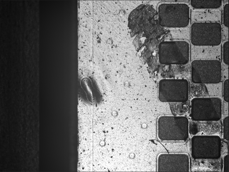
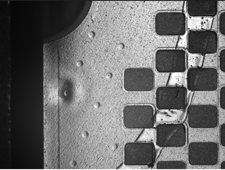
2D檢量測系統
興城提供不同精度的2D檢量測方案,提供半導體與封裝製程中,任何需要進行2D檢測的缺陷。
系統特性
- 超高解析度與高產能檢測。
- 量測精度:≥ ±1 微米(µm)。
- 即時檢測,防止良率損失。
- 數據精準量化,降低誤判。
- AI 智能判別選配,強化自動化檢測。
- 客製化設備結構配置規劃。
適用場域
- 任何物件外觀缺陷檢量測。
2D AOI measuring System
We offer a wide range of high-precision 2D inspection systems tailored for semiconductor and OSAT production lines. Designed to detect surface defects across all critical process stages.
System Features
● Ultra-high-resolution and high-throughput inspection.
● Dimensional accuracy: ≥ ±1 μm.
● Real-time inspection to prevent yield loss.
● Quantitative defect analysis to minimize false positives.
● AI-assisted defect classification to boost automation.
● Fully customizable configurations and equipment layout.
Applications
● Applicable to any component requiring dimensional or appearance validation.