

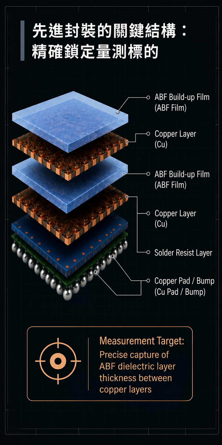
In advanced packaging and multi-layer build-up processes, tool stability and metrology accuracy depend not only on the inspection system itself, but are also closely tied to interlayer material structures, copper layer alignment, high-frequency dielectric thickness control, measurement precision, and manufacturing yield enhancement. Accurately targeting and measuring ABF Film thickness is critical to ensuring signal transmission integrity and structural stability in high-end chip packaging.
Leveraging specialized optical metrology and proprietary algorithm development capabilities, Centrum Technology delivers customized high-precision advanced packaging metrology systems tailored to customer product specifications, multi-layer stack-ups, and inspection demands. These include ABF Film dielectric layer metrology modules, copper layer thickness profiling, and multi-layer micron-level thickness analysis tools. Specifically, the ABF dielectric layer metrology module accurately locks onto and captures the ABF dielectric thickness between multiple copper layers, satisfying micron-level precision demands and supporting advanced IC substrates as well as 3D advanced packaging metrology applications.
This capability demonstrates Centrum Technology’s strength not merely as a hardware provider, but in seamlessly integrating multi-layer film thickness measurement, visual feature recognition, optical interferometry, and precision substrate alignment design to help customers build stable and dependable high-volume manufacturing inspection solutions.
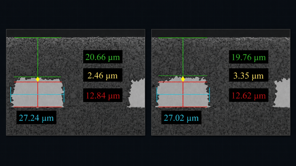
- Ultra-High-Precision Layer Thickness Metrology: Accurately isolates multi-layer structures with micron-level mechanical and optical measurement accuracy.
- Deep Multi-Layer Structural Profiling: Supports comprehensive metrology for ABF build-up films, copper layers, and structural features.
- Cross-Sectional Micron Data Visualization: Delivers real-time quantification of interlayer interface features to achieve inline process monitoring.