

In advanced packaging processes, critical defects such as inner cracks, chipping, overlay shift, and embedded foreign particles within the die are completely concealed beneath the surface. Relying solely on conventional surface AOI creates severe inspection blind spots, compromising downstream process validation and high-volume manufacturing (HVM) yield.Leveraging the physical transmission characteristics of infrared light through silicon.
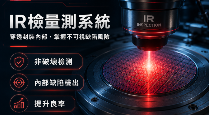
Centrum Technology IR Metrology & Inspection System is dedicated to deep, non-destructive inspection of silicon wafers and dies. Without sample destruction, the system achieves precise internal structural characterization, defect depth profiling, and in-line process quality control—drastically shortening root-cause traceability cycles and maximizing defect disposition efficiency.
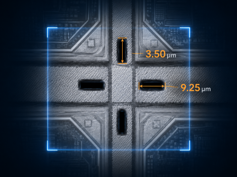
- Advanced Short-Wave Infrared (SWIR / IR) Silicon Penetration Technology
- 100% Non-Destructive Testing (NDT): Zero damage to wafer samples.
- High-Resolution Sub-Surface Structural Imaging, Defect Characterization & In-Line Quality Control