

Semiconductor:2D Laser Line Profiler System
High-Resolution 2D AOI: Precision Tracking of Surface Defects and Dimensional Drift
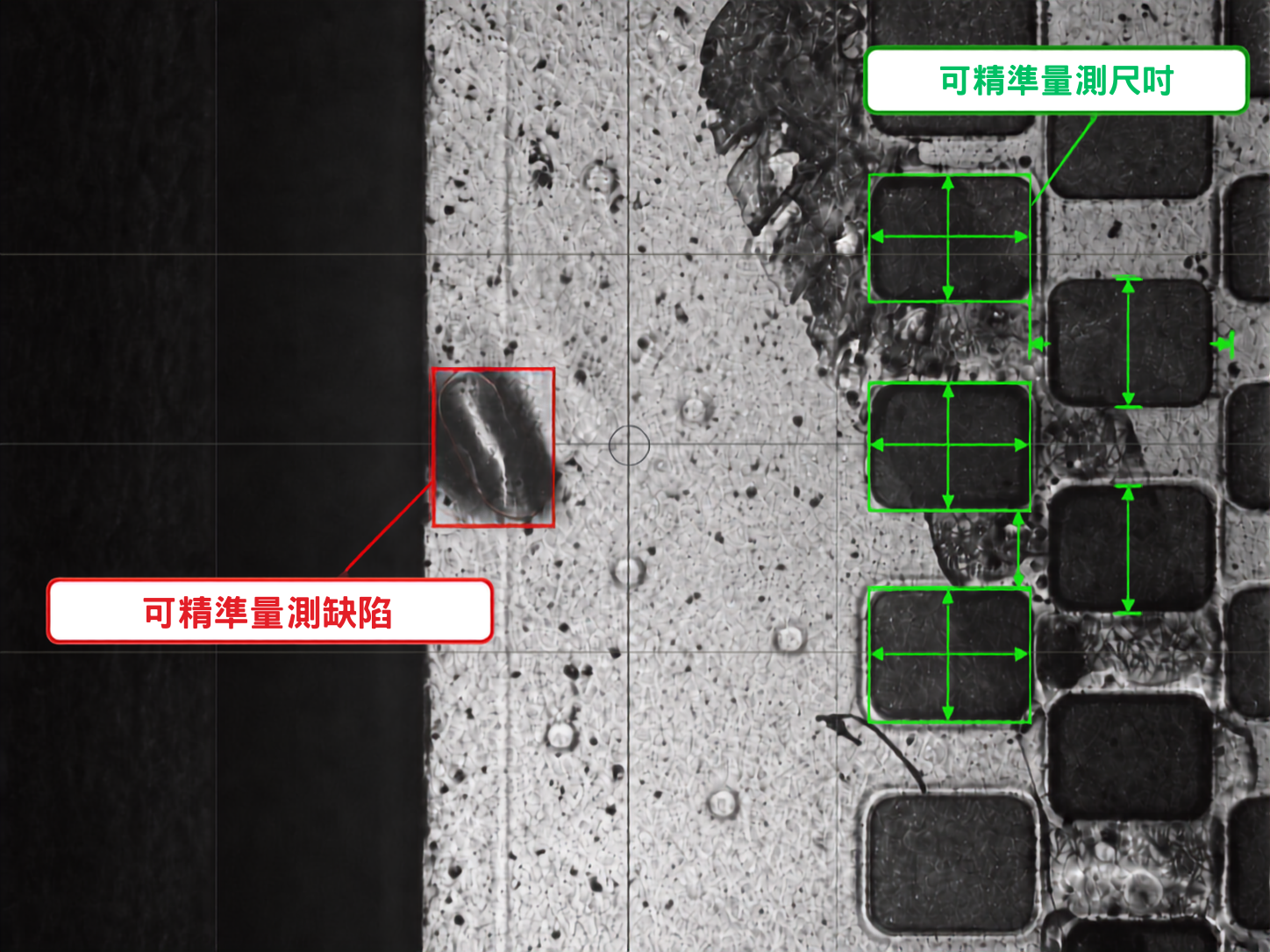
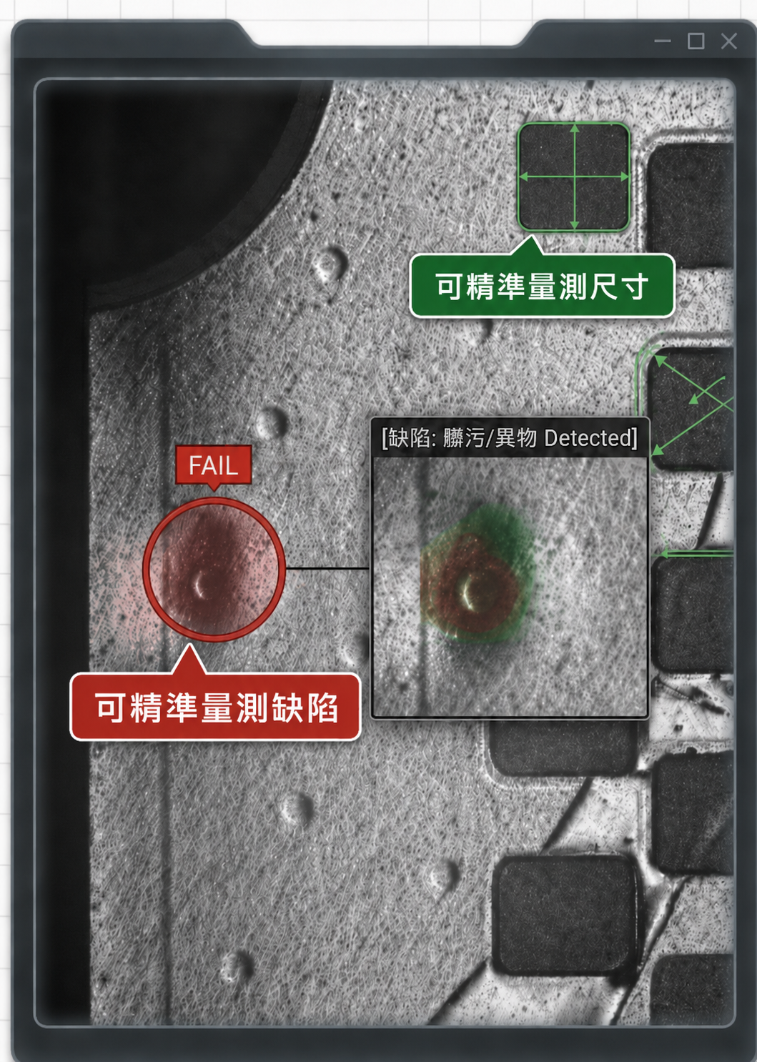
Centrum Technology’s 2D inspection and metrology solution combines high-resolution optical inspection with precision dimensional measurement to detect surface defects, dimensional shifts, pattern abnormalities, and other critical visual anomalies. Real-time quantitative analysis enables consistent defect classification and critical dimension monitoring across semiconductor and advanced packaging processes.
Designed for high-volume manufacturing and process development, the solution helps reduce over-kill and under-kill, improve inspection consistency, accelerate process optimization, and strengthen overall yield and quality control.
Core Technology Highlights
- Ultimate Precision Metrology: Measurement accuracy ≥ ±1 µm.
- Real-Time Inspection Engine: Harmonizes ultra-high optical resolution with class-leading throughput.
- Optional AI Intelligent Classification Module: Reinforces automated inline defect classification and screening accuracy.