

Semiconductor:3D Laser Solution: Underfill Inspection System
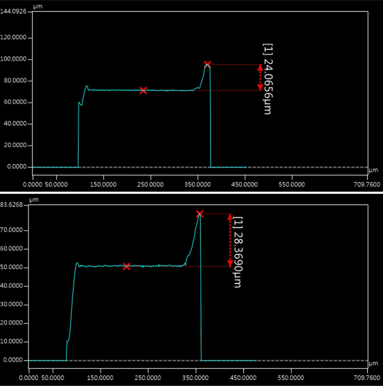
Centrum Technology’s 3D laser inspection and metrology solution provides high-precision measurement of underfill profiles, warpage, bump height, coplanarity, wire-bond loop height, and other critical 3D structures, with Z-axis accuracy down to 1 µm. Real-time cross-sectional profiling and 3D surface mapping enable quantitative analysis of structural variation and process abnormalities.
Designed for advanced packaging and semiconductor assembly processes, the solution supports sampling and 100% inline inspection, helping improve process stability, reduce false calls, shorten analysis cycles, and enhance assembly yield through data-driven quality control.
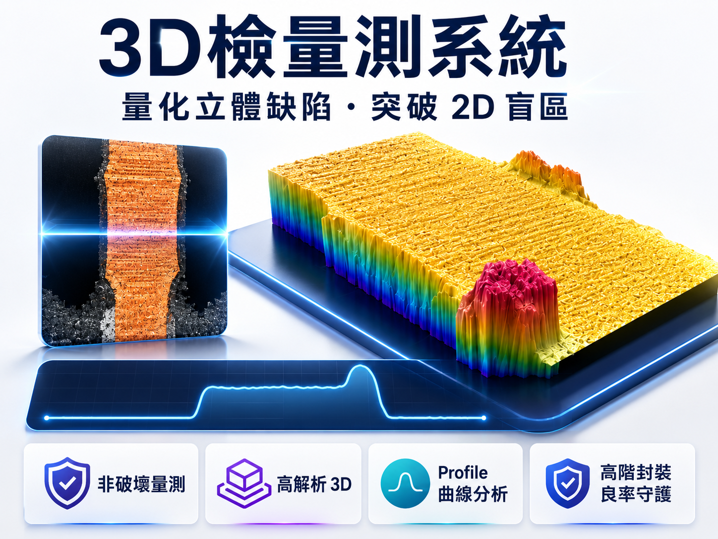
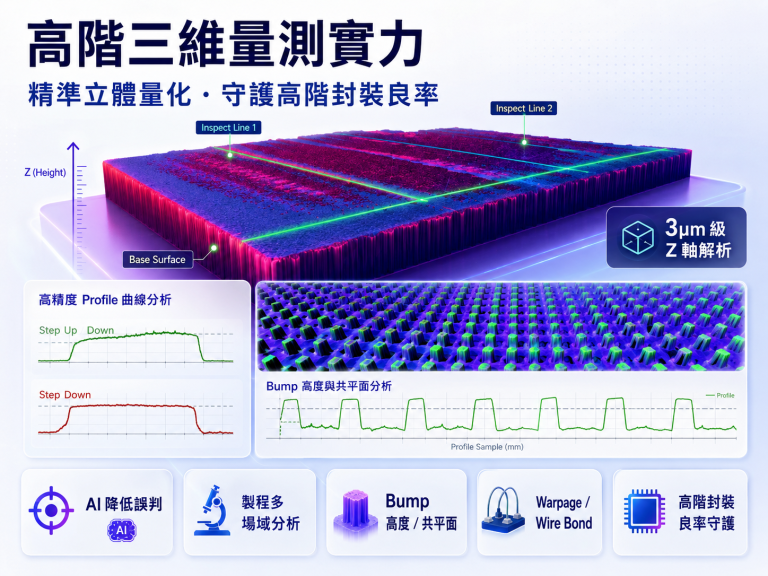
- Industrial-Grade 3 µm-Level Z-Axis Ultra-High Resolution Metrology Accuracy
- Precision Warpage Inspection for Large Dies & Substrates (Scan Area: 100 mm × 120 mm)
- Non-Destructive Inspection (NDI): Enables flexible sampling to full-inspection strategies without product scrap.
- Real-Time 3D Defect Detection: Instant visualization of cross-sectional profiles and 3D surface topography.
- Die & Substrate Warpage Profile Classification: Optimizes component compatibility during assembly.
- Optional AI-Powered Classification System: Drastically enhances automated defect recognition capabilities.
High-Flexibility, Customizable Tool Architecture & Modular Configuration