

Semiconductor – CoWoS / CoPoS 2D/3D Thickness & Coverage Inspection and Metrology
Pioneering AI Metrology in Advanced Packaging: Realizing 2D+3D Wafer and Substrate Flux Thickness Metrology
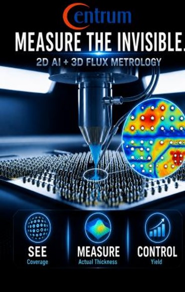
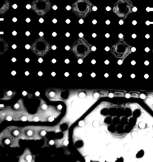
Centrum Technology’s 2D/3D flux inspection and metrology solution combines AI-powered coverage analysis with high-precision 3D thickness measurement for wafers and advanced substrates. It enables quantitative evaluation of flux coverage, thickness, and surface topography, helping identify process variation and warpage-related risks before bonding.
Designed for CoWoS, CoPoS, and advanced packaging processes, the solution supports process optimization, yield improvement, and closed-loop quality control by providing comprehensive metrology data for dispensing and bonding process verification.
Core Technology Highlights
- Exclusive 2D+3D Integrated Metrology: The industry’s only flawless solution combining 2D flux coverage analysis (AI Intelligence) with 3D thickness metrology.
- Nanometer-Scale 3D Metrology: Utilizing advanced Spectral Confocal technology with a Z-axis resolution of less than 100 nm, accurately characterizing semi-transparent thin films and minute thickness variations.
- AI-Powered 2D Coverage Intelligence: Patented multi-directional illumination combined with grayscale threshold algorithms automatically executes multi-level pad submergence classification, precisely quantifying pad coverage and spatial distribution characteristics.
- Closed-Loop & Inline Process Optimization: Metrology data can be dynamically fed back to dispensing/jetting equipment for real-time parameter tuning. Fully equipped with SECS/GEM and EFEM smart manufacturing integration capabilities, completely satisfying inline production demands.